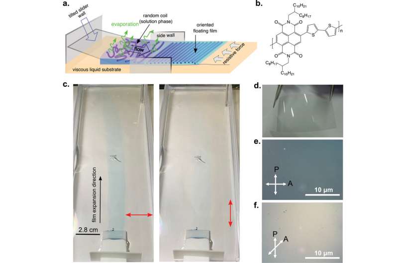
Flexible semiconductors are essential for future wearable electronics technologies, but have been difficult to integrate into complex architectures. Now, in a study recently published in Advanced Electronic Materials, researchers from Japan have developed a straightforward means of fabricating high-quality soft semiconductors for advanced electrical circuits.
Modern integrated circuit technology depends on basic elements known as complementary metal oxide semiconductor (CMOS) circuits. Silicon is the semiconductor component of most modern CMOS technology. However, because future CMOS circuits must (for example) mold to the shape of a body or integrate into clothing, much work has focused on developing soft, flexible, polymer-based semiconductors.
Several technical challenges must be overcome to integrate such semiconductors, especially n-type ones which flows electrons, into CMOS circuits. For example, preparing high-quality, layer-by-layer structures—important for CMOS device functionality—tends to be rather slow and challenging. Solving these challenges is the problem that researchers from Nara Institute of Science and Technology (NAIST) sought to address.
“Ideally, one would be able to deposit polymer films onto liquid substrates for ease of transfer to any other substrate,” explains Manish Pandey, lead author. “Our strategy offers superior control over the resulting semiconductor film morphology, which is critical to the electrical properties, compared with conventional solution processing.”
This work is based on unidirectional floating film transfer. By using a liquid substrate that does not dissolve the polymer, a solvent-dissolved polymer can be added dropwise onto the substrate, in a manner that forms a one-dimensional floating polymer film. Upon evaporation of the solvent, the polymer molecules orient perpendicular to the length direction of the film. This molecular morphology optimizes the electrical properties of the polymer film. Once the film solidifies, one can easily transfer it onto another substrate—e.g., for layer-by-layer deposition.
“We prepared an n-channel transistor that exhibited nearly no threshold voltage, which is important for maintaining power efficiency,” says Masakazu Nakamura, senior author. “By using our approach, preparing and integrating n-channel as well as p-channel transistors into one device—based on flexible semiconductors—should be straightforward.”
This work succeeded in preparing one-dimensional, polymer-based semiconductor films in an inexpensive manner that is straightforward to replicate. The NAIST researchers’ polymer film assembly methodology will be useful for advancing the prospects of flexible electronics, and helping to find replacements for silicon in upcoming wearable CMOS technology.
Manish Pandey et al, Unidirectionally Aligned Donor–Acceptor Semiconducting Polymers in Floating Films for High‐Performance Unipolar n ‐Channel Organic Transistors, Advanced Electronic Materials (2022). DOI: 10.1002/aelm.202201043
Provided by
Nara Institute of Science and Technology
Citation:
Easy fabrication of next-generation, super-flexible electronic circuits (2023, January 4)
retrieved 4 January 2023
from https://techxplore.com/news/2023-01-easy-fabrication-next-generation-super-flexible-electronic.html
This document is subject to copyright. Apart from any fair dealing for the purpose of private study or research, no
part may be reproduced without the written permission. The content is provided for information purposes only.
Stay connected with us on social media platform for instant update click here to join our Twitter, & Facebook
We are now on Telegram. Click here to join our channel (@TechiUpdate) and stay updated with the latest Technology headlines.
For all the latest Technology News Click Here
For the latest news and updates, follow us on Google News.
