Over the past decades, engineers have created increasingly advanced and highly performing integrated circuits (ICs). The rising performance of these circuits in turn increased the speed and efficiency of the technology we use every day, including computers, smartphones and other smart devices.
To continue to improve the performance of integrated circuits in the future, engineers will need to create thinner transistors with shorter channels. Down-scaling existing silicon-based devices or creating smaller devices using alternative semiconducting materials that are compatible with existing fabrication processes, however, has proved to be challenging.
Researchers at Purdue University have recently developed new transistors based on indium oxide, a semiconductor that is often used to create touch screens, flatscreen TVs and solar panels. These transistors, introduced in a paper published in Nature Electronics, were fabricated using atomic layer deposition, a process that is often employed by transistor and electronics manufacturers.
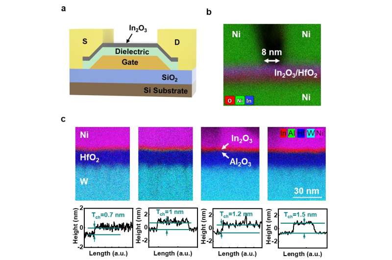
“In our recent paper, we were able to aggressively scale transistors introduced in previous works,” Peide Ye, one of the researchers who carried out the study, told TechXplore. “For example, we realized channel thickness as small as 0.5 nm, channel length as short as 8 nm, EOT as small as 0.86 nm. With all the scaling we demonstrated, we can realize a transistor delivering drain current of 3.1 mA/um at drain voltage of 0.5 V.”
Atomic layer deposition is the primary technique used to fabricate transistors with atomic-layer thin channels and dielectrics. It is a chemical-based self-limiting method that allows engineers to deposit thin films of materials onto a given substrate at atomic layer accuracy.
In their study, Ye and his colleagues used atomic layer deposition to deposit thin indium oxide films on a substrate and create highly performing transistors. These transistors have channel lengths of 8 nm and thicknesses of 0.5nm. In the future, they could potentially be integrated into a variety of existing and newly developed devices, allowing engineers to reduce their size and improve their performance.
“The ultra-low contact resistance and scaled device make the unprecedented drain current possible on BEOL compatible oxide semiconductor transistors,” Ye explained. “With more optimization and creative engineering, it is possible to deliver drain currents of 10 mA/um or even 20 mA/um.”
So far, Ye and his colleagues have primarily evaluated the transistors they created within a laboratory setting. In their next studies, however, they would like to explore their actual compatibility with current manufacturing technologies and assess their potential for real-world applications further.
“We are now interested in achieving a record performance with our transistors,” Ye added. “In addition, we plan to start exploring our new device’s potential in the real-world and look at the manufacturing technology necessary to enable its large-scale implementation.”
Researchers realize vertical organic permeable dual-based transistors for logic circuits
Mengwei Si et al, Scaled indium oxide transistors fabricated using atomic layer deposition, Nature Electronics (2022). DOI: 10.1038/s41928-022-00718-w
© 2022 Science X Network
Citation:
An indium oxide-based transistor created using atomic layer deposition (2022, March 17)
retrieved 17 March 2022
from https://techxplore.com/news/2022-03-indium-oxide-based-transistor-atomic-layer.html
This document is subject to copyright. Apart from any fair dealing for the purpose of private study or research, no
part may be reproduced without the written permission. The content is provided for information purposes only.
Stay connected with us on social media platform for instant update click here to join our Twitter, & Facebook
We are now on Telegram. Click here to join our channel (@TechiUpdate) and stay updated with the latest Technology headlines.
For all the latest Technology News Click Here
For the latest news and updates, follow us on Google News.
