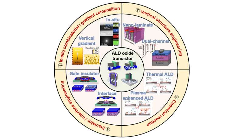
A group of scientists from Hanyang University has published a report reviewing and discussing the outlook for atomic layer deposition (ALD) based oxide semiconductor thin film transistors (TFTs). The team’s findings, which were published in the International Journal of Extreme Manufacturing, suggest that there are four benefits of ALD for TFTs based on oxide semiconductor channel layers.
Oxide semiconductor materials have gained attention as the channel layer for TFTs, and research in this area has significantly increased in recent years. Since the first report of amorphous In-Ga-Zn-O (a-IGZO) in 2003, there has been a growing interest in oxide semiconductor channel-based TFTs in the industry. Over the last 15 to 20 years, commercial displays that utilize oxide semiconductors have become ubiquitous in our daily lives.
Recently, the memory industry has shown increased interest in oxide semiconductor channels, marking the beginning of a new era in this field. The team of scientists from Hanyang University have released the report that includes a review and outlook of ALD based oxide semiconductor TFTs. They introduce the history of oxide semiconductor TFTs in display and memory industries, several recent studies related to four benefits that explain why ALD-oxide semiconductor TFTs have become industrially important, and remaining challenging issues which need to be overcome.
Representative reports of each benefit in this review indicate the main differences between ALD-deposited oxide semiconductors compared to conventionally deposited ones. The authors suggest that the values of ALD for the development and application of oxide semiconductor are as follows:
- In-situ composition control in vertical distribution: ALD enables the development of various oxide semiconductors through (a) composition control for multi-component oxide semiconductors and (b) gradient distribution of cation composition through cycle design. The metal cations constituting the multi-component oxide semiconductor can each play different roles (as carrier suppressors, carrier generators, and structure stabilizers), and their electrical properties are controlled by their distribution.
- Vertical structure engineering: ALD is very suitable for designing vertical-channel structures with enhanced interface characteristics because it enables nano-scale control and in-situ processing for dissimilar material deposition. Based on the ALD sequence, superlattice formation is possible, using nano-laminates of semiconductors and insulator, and dual-channel modulation is possible by forming heterogeneous junctions between oxide semiconductors of different compositions.
- Chemical reaction and film properties: Since the ALD method is based on a self-limiting chemical reaction, the precursor and reactant inevitably affect the characteristics of the thin film. Therefore, in ALD, it is important to select an appropriate precursor and a reactant, and different properties can be realized even with the same material.
- Insulator and interface engineering: The interface between a semiconductor and insulator is closely correlated with electrical characteristics and reliability in oxide semiconductor-based TFTs. ALD is an optimal process for improving the film quality of the interface between insulators and semiconductors and controlling the diffusion of impurities, such as hydrogen and carbon, in insulators. Furthermore, studies on the application of functional insulators and interface tailoring processes based on ALD are actively in progress.
Challenging issues remain that prevent the expansion of oxide semiconductors and their use in display and memory industry. The scaling down of devices requires thinner active materials, down to sub-nanometer thicknesses. ALD-based indium oxide can be used to drive device thickness down to 1 nm, and further research is necessary to develop this method as an ultra-thin active layer for scaling down.
The fabrication of three-dimensionally (3D) structured devices such as gate-all-around (GAA)-TFT, channel all around (CAA)-TFT, and vertical (V)-TFT is challenging but will broaden the industrial applications of ALD oxide semiconductors. When applied as an active layer in a 3D structure, they can increase the degree of integration, and monolithic 3D integration, by stacking TFTs in the vertical direction.
Also, achieving non-comparable paired p-type oxide semiconductors is another task for the scalability of oxide semiconductors, in CMOS inverters. The commercialization of ALD-oxide semiconductors is still ongoing. We believe that the suggested benefits of ALD for oxide semiconductors will motivate efforts to address the remaining challenges in 3D-structured, very thin devices, CMOS inverters, and future applications.
From the history of oxide semiconductor TFTs to remained challenging issues, researchers try to provide the insight into how can we achieve desired performance with ALD process and what we need to overcome to expand this in the future developed industry to the other researchers in this field.
Professor Jin-Seong Park, who is the leader of the research team, commented, “Study on the practical use of oxide semiconductor has become important not only in the display but also memory/logic semiconductor field. We summarized and organized the reported research over the past 15 years by our group (Hanyang University) as well as the other leading groups about ALD-based oxide semiconductor TFT application. We believe that our suggestion of 4-main keywords and what we need to do to overcome for future applications in the industry could be a valuable perspective for worldwide researchers on this field.”
More information:
Hye-Mi Kim et al, Atomic layer deposition for nanoscale oxide semiconductor thin film transistors: review and outlook, International Journal of Extreme Manufacturing (2023). DOI: 10.1088/2631-7990/acb46d
Provided by
International Journal of Extreme Manufacturing
Citation:
Review and outlook of atomic layer deposition for nanoscale oxide semiconductor thin film transistor (2023, February 22)
retrieved 22 February 2023
from https://techxplore.com/news/2023-02-outlook-atomic-layer-deposition-nanoscale.html
This document is subject to copyright. Apart from any fair dealing for the purpose of private study or research, no
part may be reproduced without the written permission. The content is provided for information purposes only.
Stay connected with us on social media platform for instant update click here to join our Twitter, & Facebook
We are now on Telegram. Click here to join our channel (@TechiUpdate) and stay updated with the latest Technology headlines.
For all the latest Technology News Click Here
For the latest news and updates, follow us on Google News.
